 作者投稿
作者投稿 专家审稿
专家审稿 编辑办公
编辑办公

Development of a 22 Nano Line Width Standard Based on Intrinsic SiliconLattice Constants
-
摘要: 纳米线宽作为典型纳米几何特征参量之一,其量值准确性对于先进制造等领域尤为重要。随着纳米尺度向着极小尺寸发展,测量精度要求达到亚纳米级,这给纳米线宽的精确测量带来了新的挑战。2018年第26届国际计量大会提出使用硅{220}晶面间距作为米定义的复现方式,这为原子尺度纳米线宽计量技术提供了新的思路与方法。基于多层膜沉积技术制备了22 nm内禀硅晶格的线宽标准器,采用高分辨透射电子显微镜,以标准器中的硅晶格常数为标尺实现对纳米线宽的直接测量,测量不确定度优于1 nm。Abstract: The measurement accuracy of nano line widths, a critical nano geometric characteristic parameter, is of paramount importance in fields such as advanced manufacturing. As the scale of nanotechnology continues to shrink, achieving sub-nanometer measurement accuracy presents new challenges. The 26th General Conference on Weights and Measures (CGPM) in 2018 proposed using the silicon {220} lattice spacing as a secondary realization of the meter, providing a novel approach for atomic-level nano line width measurements. In this study, a 22 nm intrinsic silicon lattice line width standard was developed using multi-layer film deposition technology. Employing high-resolution transmission electron microscopy (HRTEM), the silicon lattice constant within the standard was used as a scale for direct nano line width measurement. The measurement uncertainty achieved is better than 1 nm.
-
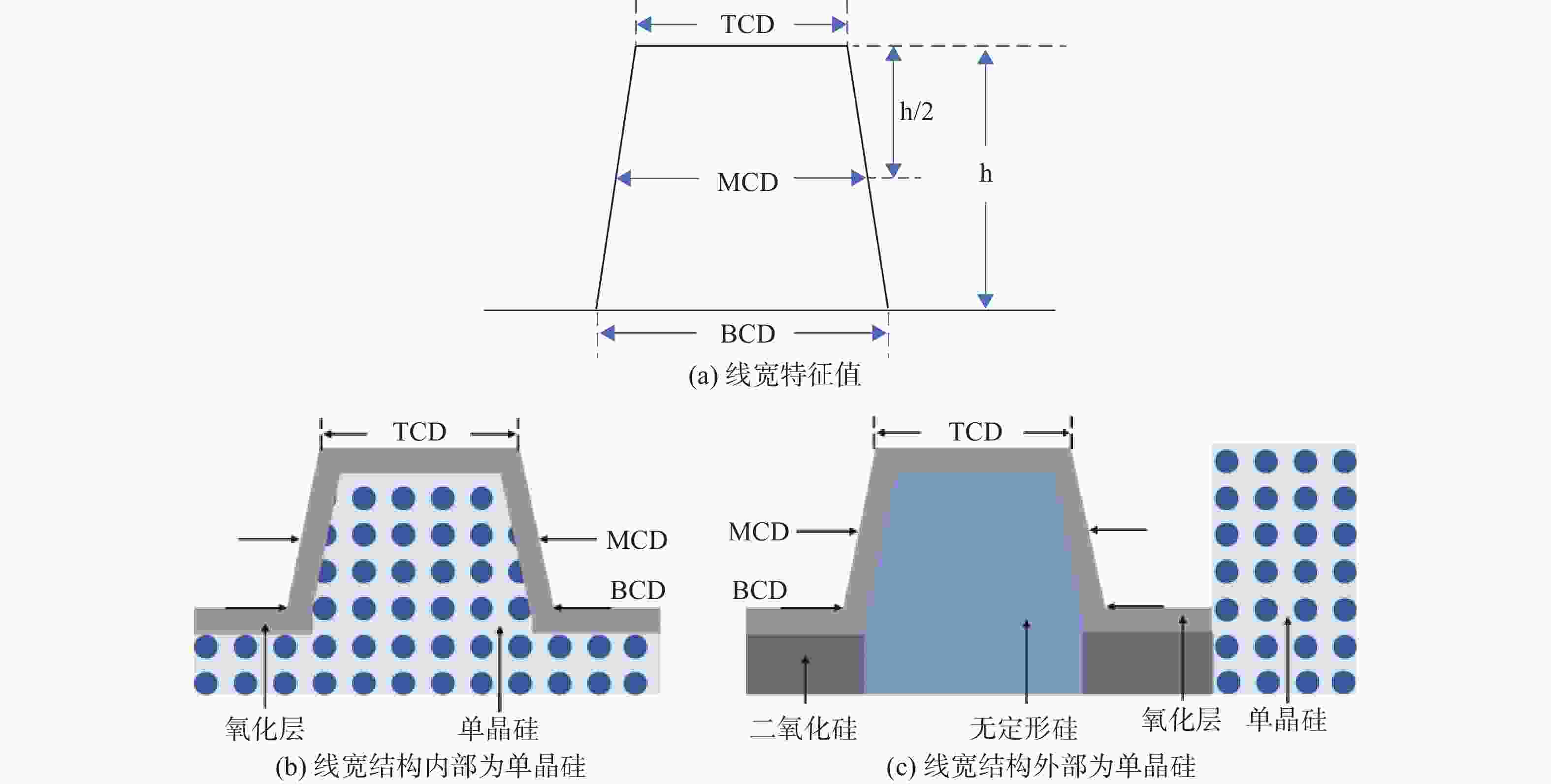
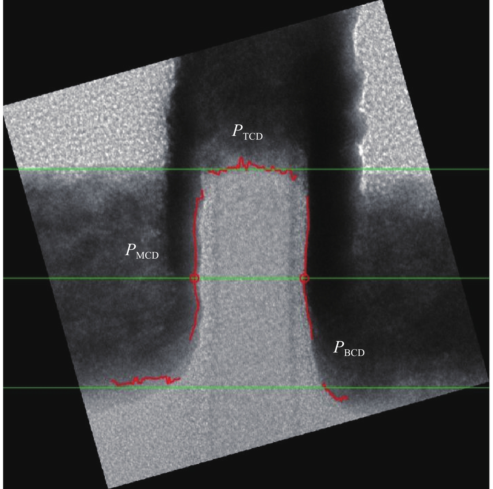
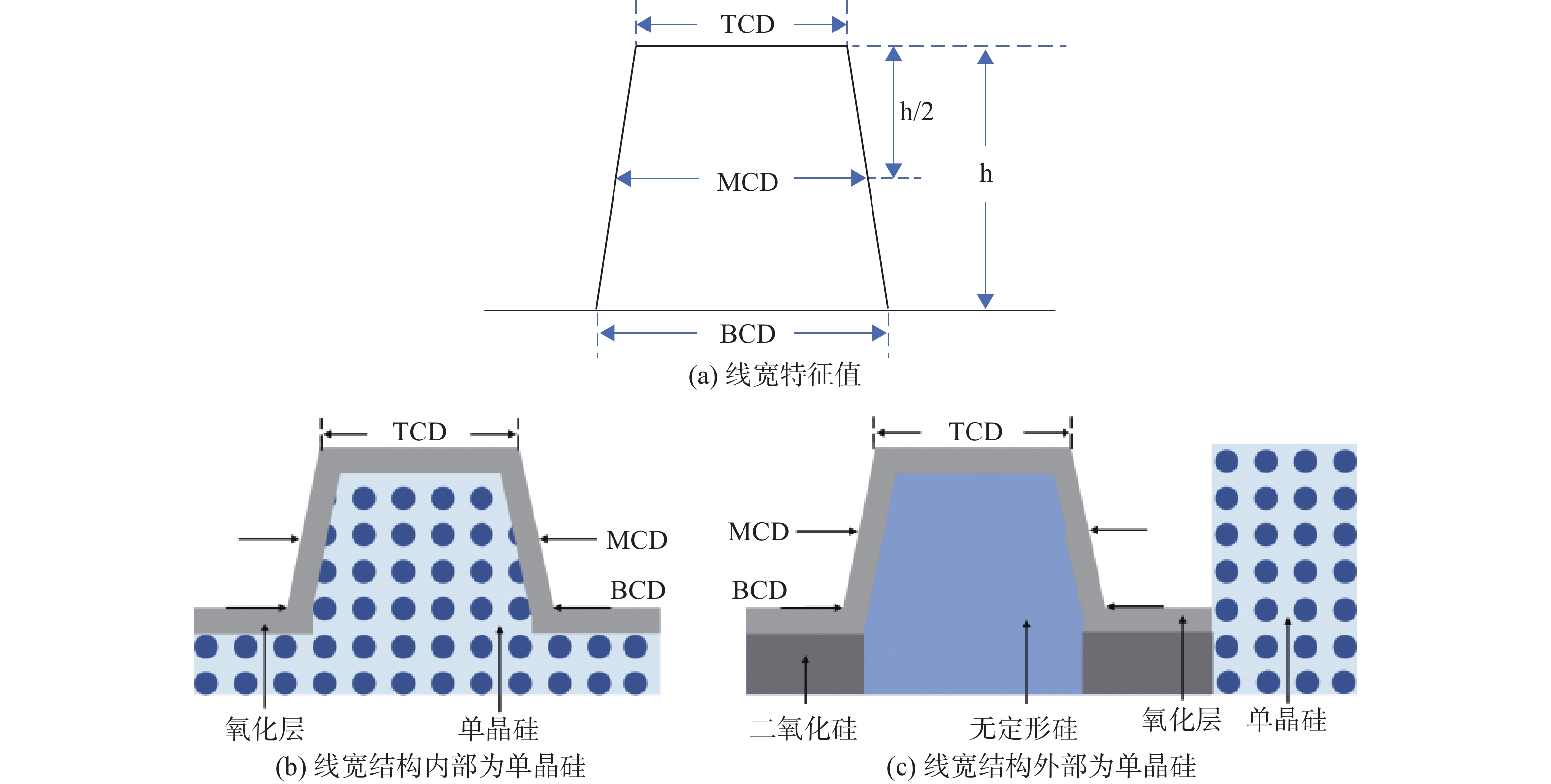
图 1 纳米线宽结构示意图:(a)线宽特征值,(b)线宽结构内部为单晶硅,(c)线宽结构外部为单晶硅
Figure 1. Nano line width structure: (a) characteristic values, (b) monocrystalline silicon inside the structure, and (c) monocrystalline silicon outside the structure

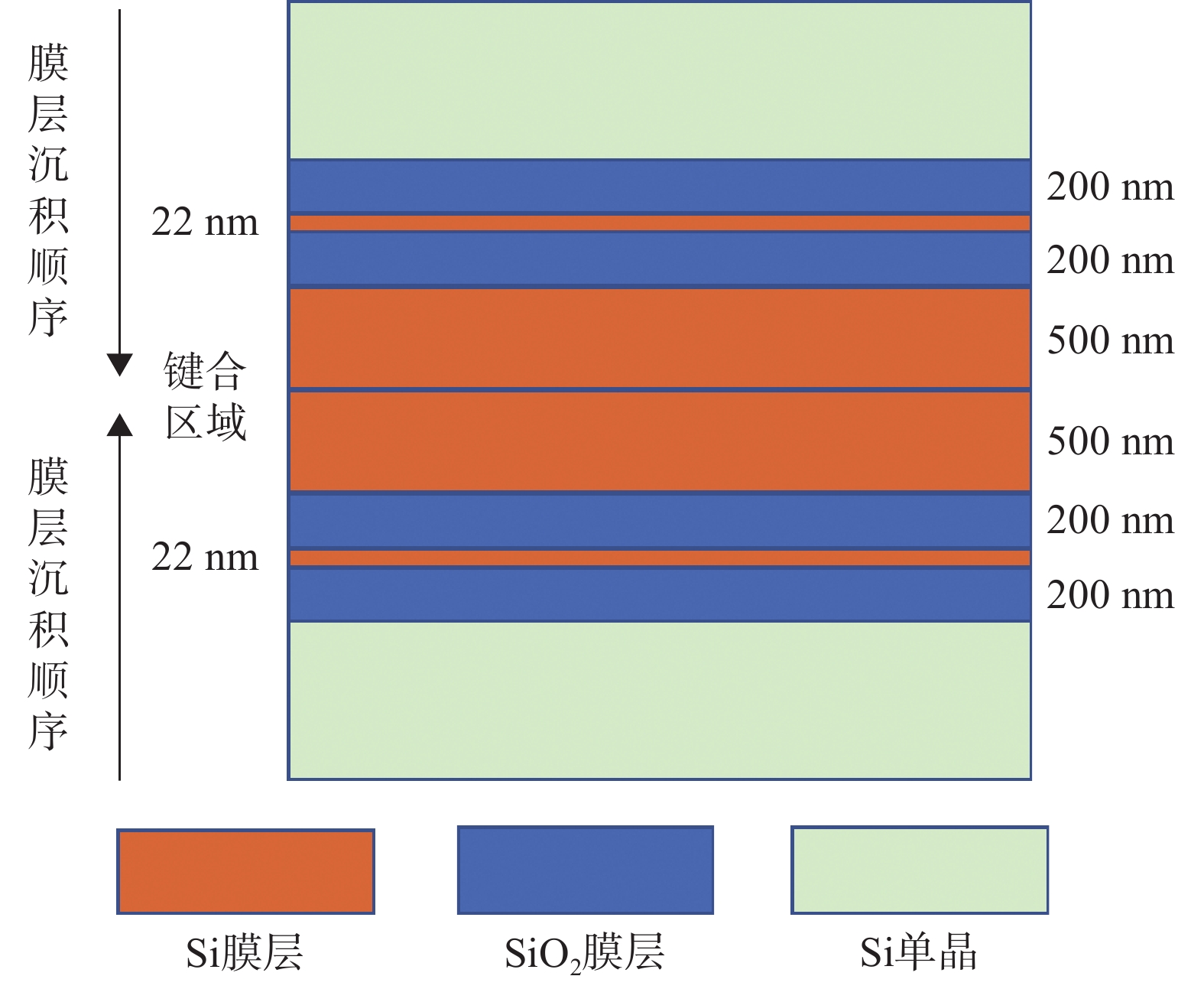
图 3 线宽标准器实物图及其扫描电子显微图像
Figure 3. Physical image of the nano line width standard and its scanning electron microscopy image
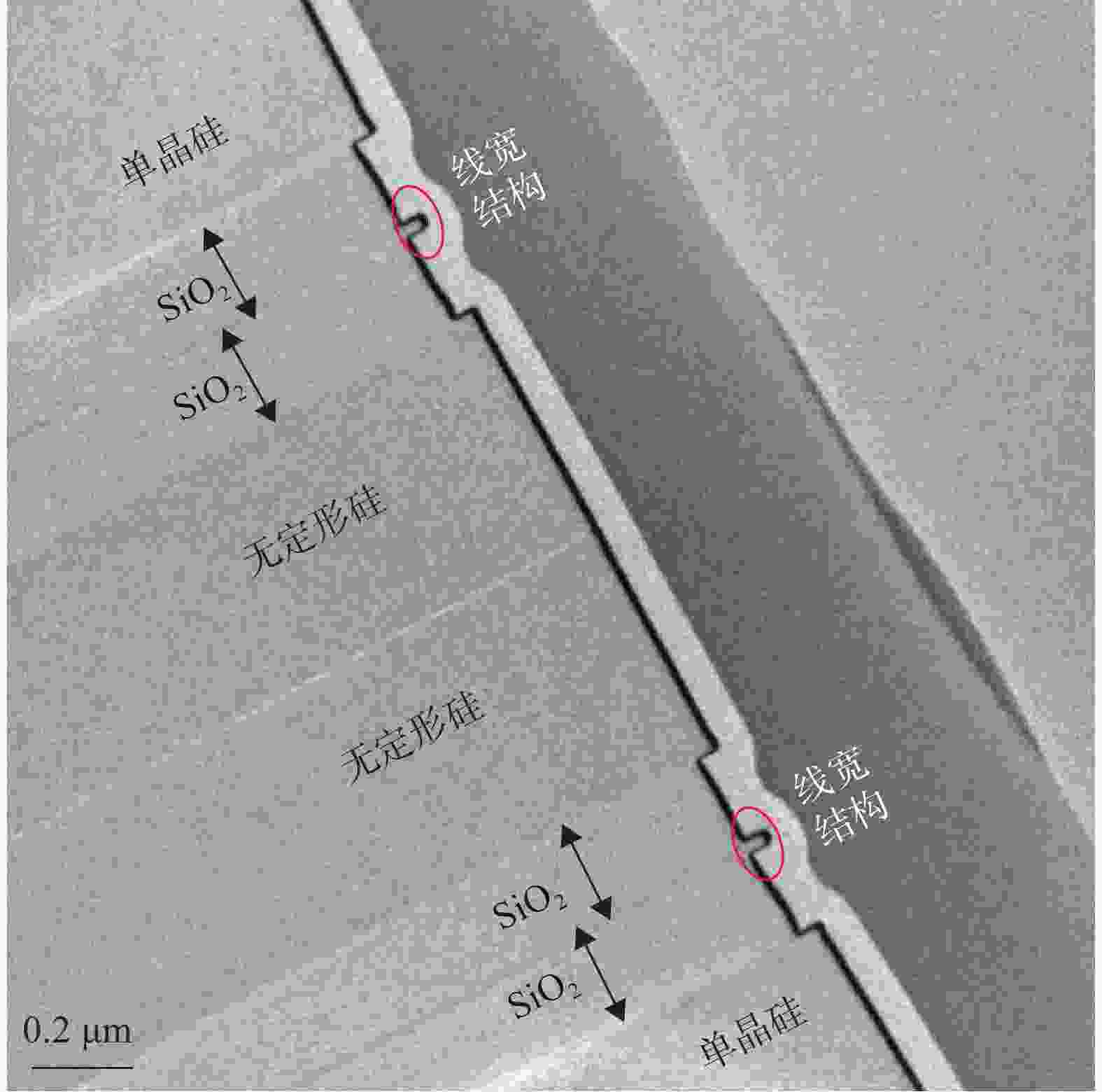
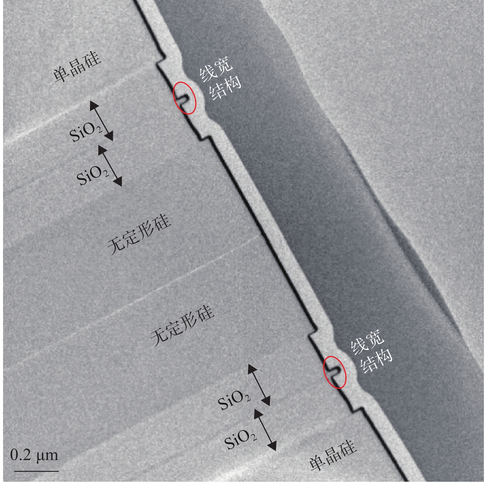
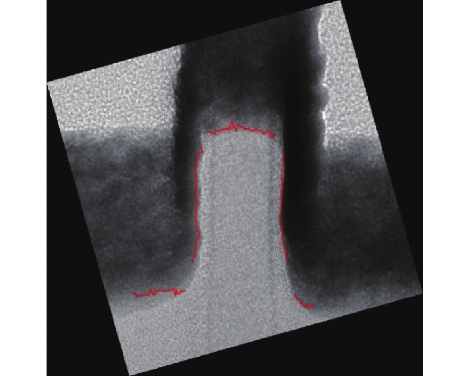
图 4 线宽的透射电子显微图像
Figure 4. Transmission electron microscope image of the nano line width
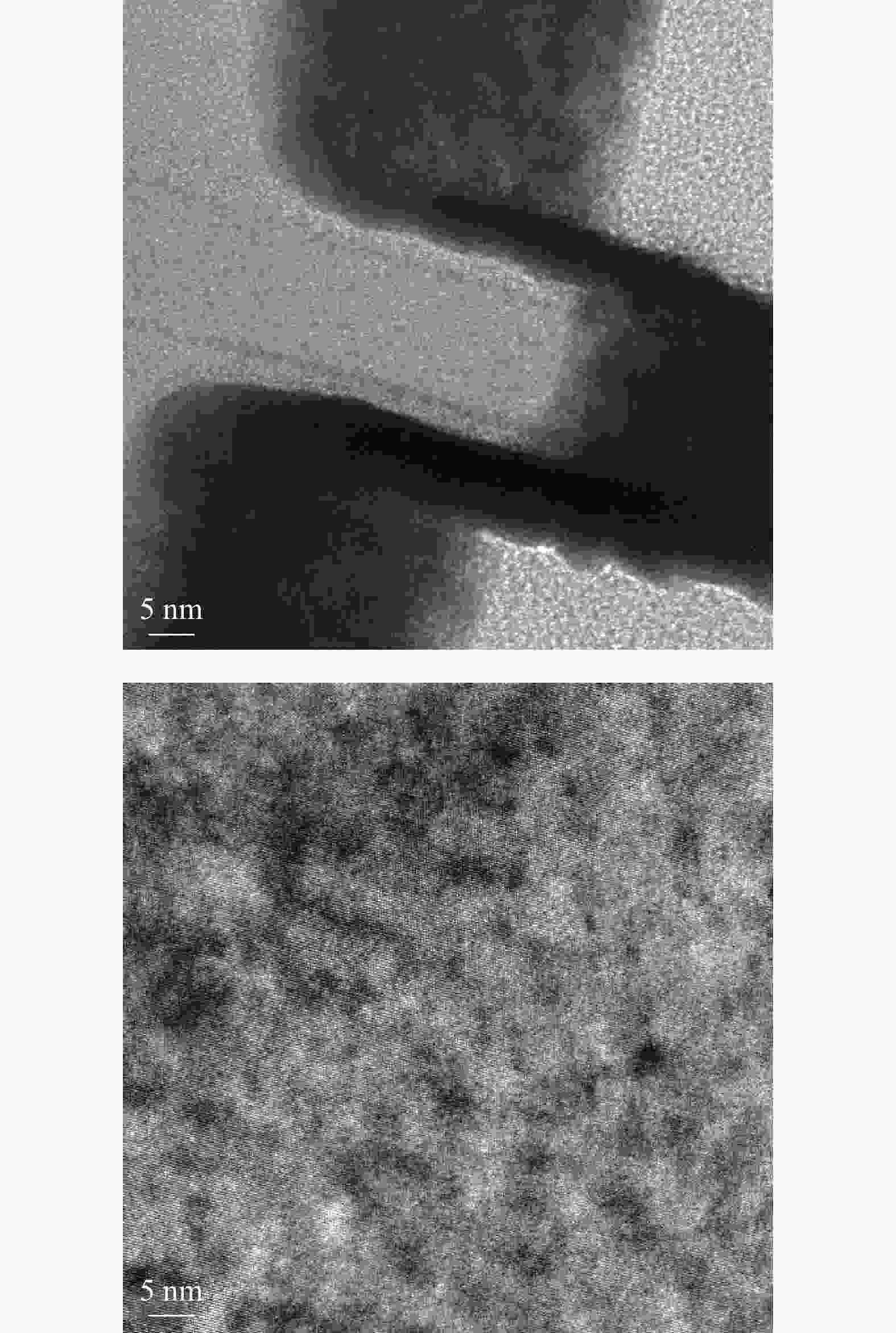
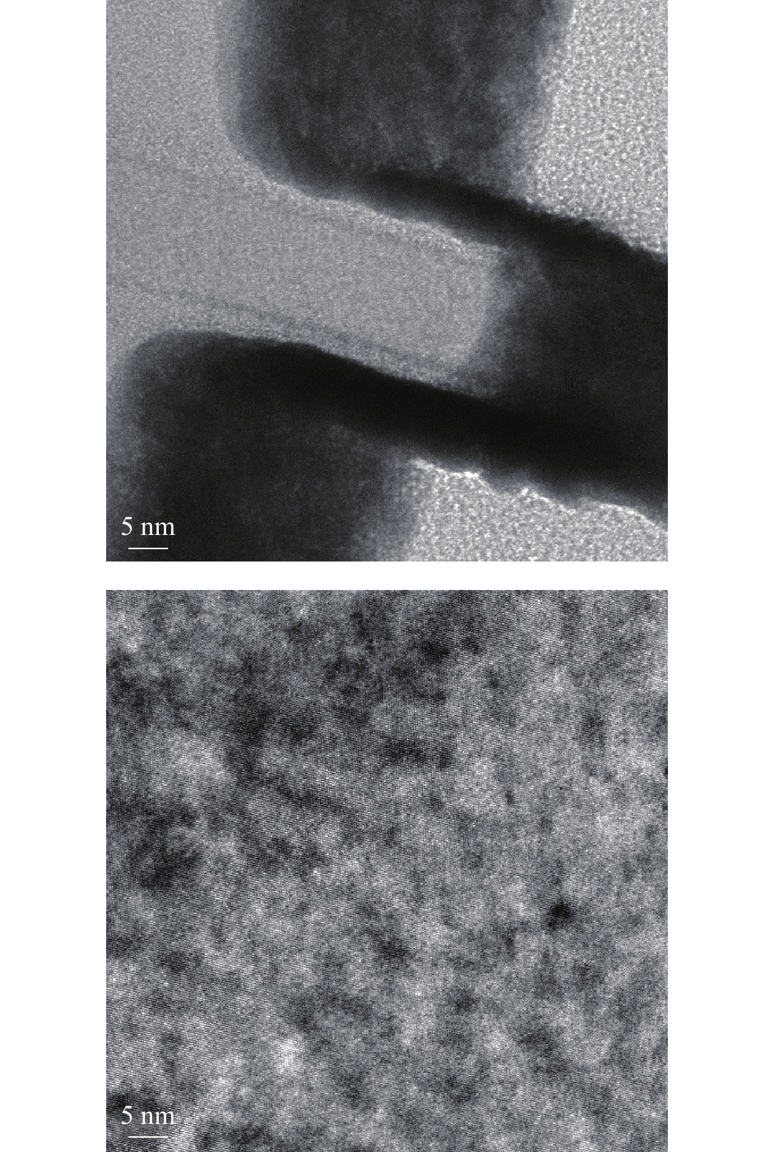
图 5 纳米线宽结构及其硅晶格的高分辨透射电子显微图像
Figure 5. High-resolution transmission electron microscope images of the nano line width structure and its silicon lattice
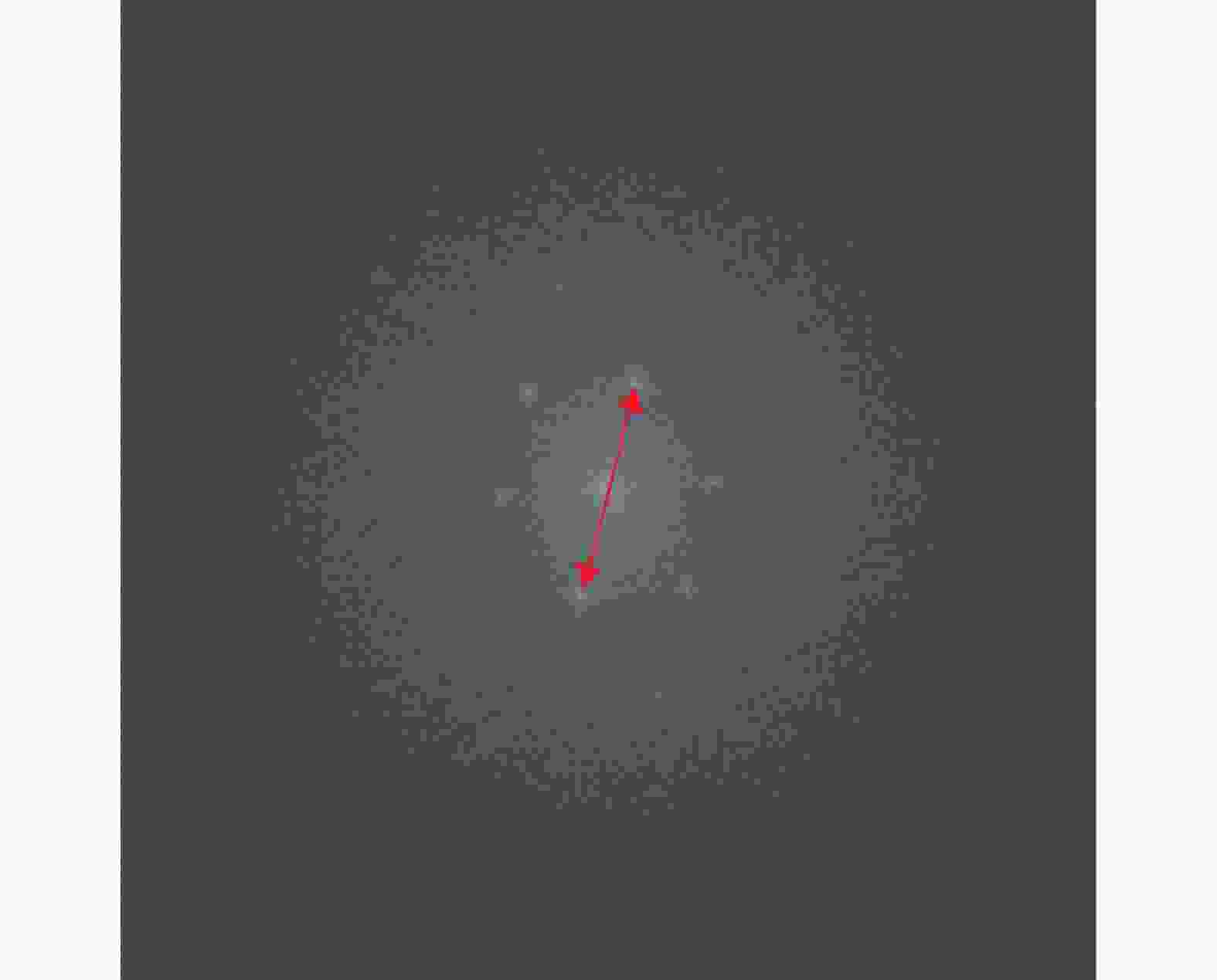
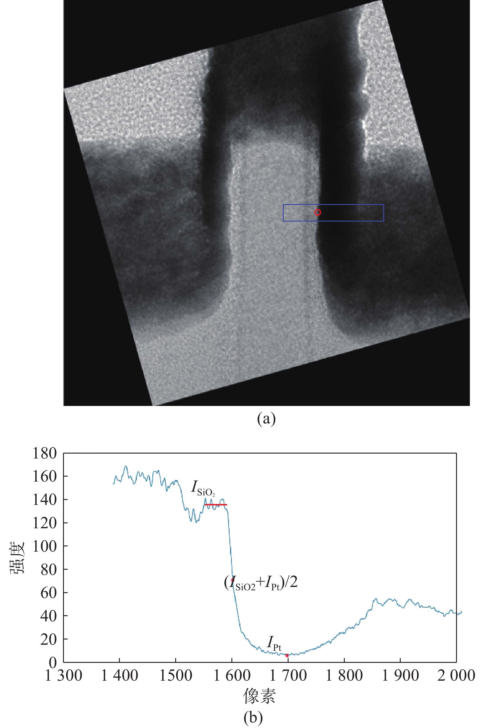
图 9 硅晶面间距像素测量过程图
Figure 9. Process diagram for measuring pixels of silicon crystal plane spacing
表 1 高放大倍率对应的视场大小
Table 1. Field size corresponding to high magnification
高放大倍率 视场大小 285 k 74.375 nm×74.375 nm 400 k 53.155 nm×53.155 nm 450 k 47.847 nm×47.847 nm 690 k 31.572 nm×31.572 nm  下载: 导出CSV
-
[1] CCL. Mise en pratique for the definition of the metre in the SI [R]. 2019. [2] CCL-GD-MeP-1. Recommendations of CCL/WG-N on: Realization of the SI metre using silicon lattice parameter and x-ray interferometry for nanometre and sub-nanometre scale applications in dimensional nanometrology [R]. 2019. [3] CCL-GD-MeP-2. Recommendations of CCL/WG-N on: Realization of SI metre using silicon lattice and Transmission Electron Microscopy for Dimensional Nanometrology[R]. 2019. [4] Wu Z R, Cai Y N, Wang X R, et al. Amorphous Si critical dimension structures with direct Si lattice calibration[J]. Chinese Physics B, 2019, 28(3): 030601. doi: 10.1088/1674-1056/28/3/030601 [5] Hoefflinger B. Chips 2020 [M]. The Frontiers Collection. Springer, Berlin, Heidelberg, 2011: 161-174. [6] E Massa, G Mana, U Kuetgens, et al. Measurement of the lattice parameter of a silicon crystal[J]. New Journal of Physics, 2009, 11: 053013. doi: 10.1088/1367-2630/11/5/053013 [7] E Massa, G Mana, U Kuetgens, et al. Measurement of the {220} lattice-plane spacing of a 28Si x-ray interferometer[J]. Metrologia, 2011, 48: S37-S43. doi: 10.1088/0026-1394/48/2/S06 [8] Luca Ferroglio, Giovanni Mana, and Enrico Massa. Si lattice parameter measurement by centimeter X-ray interferometry[J]. OPTICS EXPRESS, 16(21): 16877-16888. [9] E Massa, G Mana, and U Kuetgens. Comparison of the INRIM and PTB lattice-spacing standards[J]. Metrologia, 2009, 46(3): 249. doi: 10.1088/0026-1394/46/3/011 [10] A. Bergamin, G. Cavagnero, G. Mana, et al. Scanning X-ray interferometry and the silicon lattice parameter: towards 10−9 relative uncertainty?[J]. THE EUROPEAN PHYSICAL JOURNAL B, 1999, 9: 225-232. [11] 崔建军. 基于Fabry-Perot干涉与原子晶格间距的微位移计量及溯源研究 [D]. 天津: 天津大学, 2014. [12] Ernest G K, Szabo C I, Cline J P, et al. The lattice spacing variability of intrinsic float-zone silicon[J]. Journal of Research of the National Institute of Standards and Technology, 2017, 122: 24. doi: 10.6028/jres.122.024 [13] Gaoliang Dai, XiukunHu, and Johannes Degenhardt. Bottom-up approach for traceable calibration of tip geometry of stylus profilometer[J]. Surface Topography:Metrology and Properties, 2022, 10: 015018. doi: 10.1088/2051-672X/ac4f36 [14] Keita Kobayashi, Ichiko Misumi, and Kazuhiro Yamamoto. Experimental evaluation of uncertainty in sub- nanometer metrology using transmission electron microscopy due to magnification variation[J]. Measurement Science and Technology, 2021, 32: 095011. doi: 10.1088/1361-6501/ac03e4 [15] Harald Bosse, Bernd Bodermann, Gaoliang Dai, et al. Challenges in naonometroloy: high precision measurement of position size[J]. Technisches Messen, 2015, 82(7-8): 346-358. doi: 10.1515/teme-2015-0002 [16] R. G. Dixson, R. A. Allen, W. F. Guthrie, et al. Traceable calibration of critical-dimension atomic force microscope linewidth measurements with nanometer uncertainty[J]. Journal of Vacuum Science & Technology B, 2005, 23(6): 3028-3032. [17] Gaoliang Dai, Kai Hahm, Frank Scholze. Measurements of CD and sidewall profile of EUV photomask structures using CD-AFM and tilting-AFM[J]. Measurement Science and Technology, 2014, 25: 044002. doi: 10.1088/0957-0233/25/4/044002 [18] Dai G L, Zhu F, Heidelmann M, et al. Development and characterisation of a new line width reference material[J]. Measurement Science and Technology, 2015, 26: 115006. doi: 10.1088/0957-0233/26/11/115006 [19] Guthrie W F, Dixson R G, Allen R, et al. RM 8111: development of a prototype linewidth standard[J]. Journal of Research of the National Institute of Standards and Technology, 2006, 111(3): 187-203. doi: 10.6028/jres.111.016 [20] Orji N G, Dixson R G, Garcia-Gutierrez D I, et al. TEM calibration methods for critical dimension standards[J]. Metrology, Inspection, and Process Control for Microlithography XXI, 2007, 6518: 651810. doi: 10.1117/12.713368 [21] Dai G L, Hahm K, Bosse H, et al. Comparison of line width calibration using critical dimension atomic force microscopes between PTB and NIST[J]. Measurement Science and Technology, 2017, 28: 065010. doi: 10.1088/1361-6501/aa665b [22] 高思田, 李琪, 施玉书, 等. 我国微纳几何量计量技术的研究进展[J]. 仪器仪表学报, 2017, 38(8): 1822-1829. doi: 10.3969/j.issn.0254-3087.2017.08.001 [23] 施玉书, 李伟, 余茜茜, 等. 基于原子力显微术的5 nm台阶高度标准物质溯源与定值技术研究[J]. 仪器仪表学报, 2020, 41(3): 79-86. [24] Yushu Shi, Wei Li, Sitian Gao, et al. Atomic force microscope scanning head with 3-dimensional orthogonal scanning to eliminate the curved coupling[J]. Ultramicroscopy, 2018, 190: 77-80. doi: 10.1016/j.ultramic.2018.03.020 [25] Wang F, Shi Y S, Li W, et al. Characterization of a nano line width reference material based on metrological scanning electron microscope[J]. Chin. Phys. B, 2022, 31(5): 050601. doi: 10.1088/1674-1056/ac3225 [26] Fang Wang, Yushu Shi, Shu Zhang, et al. Automatic Measurement of Silicon Lattice Spacings in High-Resolution ransmission Electron Microscopy Images Through 2D Discrete Fourier Transform and Inverse Discrete Fourier Transform[J]. Nanomanufacturing and Metrology, 2022, 2: 119-126. [27] Joachim Mayer, Lucille A. Giannuzzi, Takeo Kamino, et al. TEM Sample Preparation and FIB-Induced Damage[J]. MRS BULLETIN, 2007, 32: 400-407. doi: 10.1557/mrs2007.63 [28] 周伟敏, 徐南华. 聚焦离子束( FIB) 快速制备透射电镜样品[J]. 电子显微学报, 2004, 23(4): 513. doi: 10.3969/j.issn.1000-6281.2004.04.211 -


 点击查看大图
计量
- 文章访问数: 118
- HTML全文浏览量: 59
- PDF下载量: 17
- 被引次数: 0

